Download the syllabus.
WEEK 1
Lecture #1: PCB Design History & The New Scheme of Things Engineering Baseline
- A brief history of PCB design methodologies and the need for something better.
- What exactly does it mean to “transform your designs.”
- Capture schematic diagrams that meet troubleshooting engineering ideals.
- Define an Special Routing Instructions (SRI) for your design to enable the beginning of the constraint process.
- Develop techniques that will transform engineering baselines for all board types.
- Understand the need for an ECAD/MCAD model leading to a PCB model database.
- Embrace producibility standards for stack-ups and DFM/A as a strict design baseline.
- Generate board design notebooks that enable stable process flow of your designs.
Lecture #2: Pre-routing schemes & Model-base Methodologies
- 7-min round table discussion on Lecture #1.
- Let’s understand ECAD/MCAD model relationships and interface tactics.
- An introduction to producibility methodologies.
- Design and understand via structures and space minimization methods.
- Apply component placement methodologies incorporating DFM/A concepts.
- Understand and adapt general and complex routing features to your designs.
- Establish local and global constraint management tools to engineer your PCB designs.
- Unify ECAD/MCAD models to deliver an engineered and producible PCB Model-based database.
WEEK 2
Lecture #3: A Sample Model to Show Us How to Transform Through Constraints
- 7-min round table discussion on Lecture #2.
- Introduction to our sample PCB Design Model.
- Schematic + Housing + Layout = PCB Design Model-based database.
- Develop and shape the mechanical model to the PCB design model.
- Learn methodologies to control the PCB Design model.
- Utilize PCB design “visions” to enable process constraint management practices.
- Understand PCB fabrication and assembly processes that maximize design constraints.
- Prioritize producibility guidelines to establish proper design flows of routing.
- Update and engineer our sample PCB Design Model.
Lecture #4: Continuing Motivation to Engineer Your Designs
- 7-min round table discussion on Lecture #3.
- Review an upper level of engineering our design methodologies and process flow.
- Establish producibility and DFE and DFM/A concepts as winning design drivers.
- Apply producibility concepts: Route to meet design engineering baselines.
- Drive an Interactive Design Review Process with your design team.
- Develop a design meeting and fabrication review process with your vendors.
- Conduct pre-final producibility and vendor check.
- Identify and address problems revealed by a mechanical check.
- Drive and develop a 2-D/3-D electronic mechanical check process.
WEEK 3
Lecture #5: Looking at All Board Types & Complex RF/COB Designs – Part One
- 7-min round table discussion on Lecture #4
- Do all board types have the same process flow and constraint methodologies?
- Identify various board design types and their common features.
- Simplify and categorize designs based on features and constraints.
- Utilize the model-based structure to engineer the grouping of board types.
- Manage mounting holes and via sizing within designated DFE groups.
- Organize the non-metal features for each design type group.
- Recognize that all board design types have specific features critical for their success.
- Develop Constraint Management rules/features for each board design type.
Lecture #6: Looking at All Board Types & Complex RF/COB Designs – Part Two
- Let’s go back to our sample model design and review the RF/COB circuits.
- Confirm the PCB design is ready for RF/COB design.
- Utilize model-base ideals to define the RF/COB baseline engineering scheme.
- Organize Strict Baselines/How-To/Guidelines to help Model RF/COB designs.
- Develop a separate design engineering skill set for complex RF and COB designs.
- Develop a process to update and fix broken RF/COB designs.
- Our RF/COB Model is broken – Let’s fix it.
- Summary and Final Thoughts.
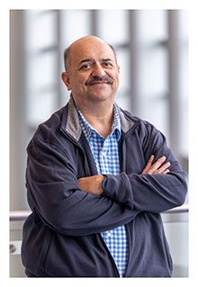
Fil Arzola
I have been blessed to work in the Engineering Design world for over 30 years, having worked in small and large companies, designing all kinds of fun stuff from hydraulic power supplies to control systems to finally making a lifetime run at designing and engineering all types of PWB board designs with a focus on complex Mixed-Signal and RF Designs. I am a graduate of the University of California, Davis, with a BSEE in Electrical and Computer Engineering. I take great pride in my work and my design passion is my greatest tool. I live in Southern California and plan to retire there as well as in Cakovec, Croatia. My second career will be writing novels and screenplays.