
Education exam and course content will be unavailable on Saturday, May 10th, from 7:00 PM to 12:00 PM CT as we perform required maintenance.
Result
Gain essential skills to design and manufacture high-quality, compliant flexible and rigid-flex printed circuit boards. Led by IPC-certified expert Nick Koop, this interactive two-week course provides a balanced foundation of theory and practical application.
Taught by an IPC-certified industry expert with more than 25 years of experience in the field, this 6-week online program introduces participants to the concepts and skills required to create real-world designs that comply with IPC standards. This introductory course will focus on front-end design concepts such as schematic capture, library parts creation, basic electrical engineering concepts, and documentaion.
In this course, participants employ the lessons learned in Introduction to PCB Design I to effectively implement their designs using techniques such as multi-layer routing, signal integrity, transmission lines, and more. The course also focuses on how manufacturing and assembly techniques impact design, documentation and manufacturing file generation.
In un settore altamente competitivo come quello dell'elettronica, le conoscenze e le competenze di chi progetta il layout del circuito stampato (PCB) e del suo assemblaggio (PBA) hanno un impatto diretto sul successo o sul fallimento del prodotto e incide sul time-to-market. Il corso online sui Fondamenti di PCB IPC è progettato per fornire le competenze necessarie per creare schemi che rispecchino accuratamente l’intento progettuale e la conformità agli standard IPC per la documentazione dello schema.
The course will start with design of HDI and advanced packaging concepts. This will be followed by embedded component design and the students will see how concepts from HDI are used in the implementation of embedded components. Next, concepts necessary for the design of wearable electronics and how the use of concepts from HDI and Embedded are necessary to achieve the small size and light weight of wearable electronics.

Taught by an industry expert with more than 40 years of experience in the field, this three-week online program is designed to provide the knowledge and skills necessary to reduce or eliminate design, documentation, and capability issues that often arise when completed PCB designs are sent to the fabricator for production.

This course addresses specific design challenges encountered in military and aerospace applications, including the effects of vibration, shock, radiation, and altitude, extended operating temperature range, and other design considerations for high reliability applications. PCB Design for Military & Aerospace Applications also focuses on the impact of these designs on manufacturing and assembly techniques, documentation, and manufacturing file generation.
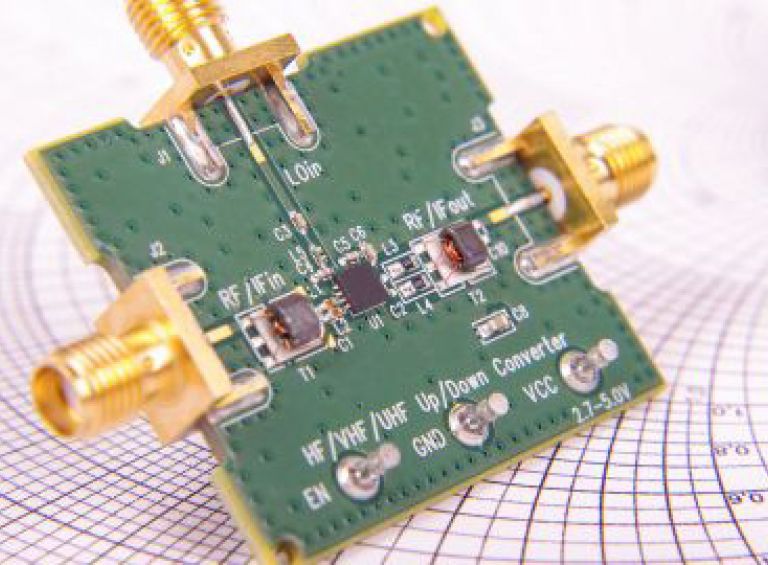
This course provides the theoretical knowledge and practical skills required to create IPC-compliant PCB designs for high-speed analog, radio (RF), and microwave frequencies. This program is designed to provide circuit board designers with a balanced foundation of theoretical knowledge and practical skills in printed circuit board design. Upon completion, participants will be able to:
Design boards for high-speed analog and RF/microwave frequencies.
Understand the trade-offs in materials used in these applications.
Define a board stackup that implements structures that will meet the needs of these designs.
Understand and mitigate signal integrity issues for these designs.
Understand and define the effects of mechanical retention needs for these applications.
Define and implement the tighter manufacturing tolerances needed for these designs.
Understand the use of mixed material stackups in these designs.
Understand the documentation requirements for these designs.
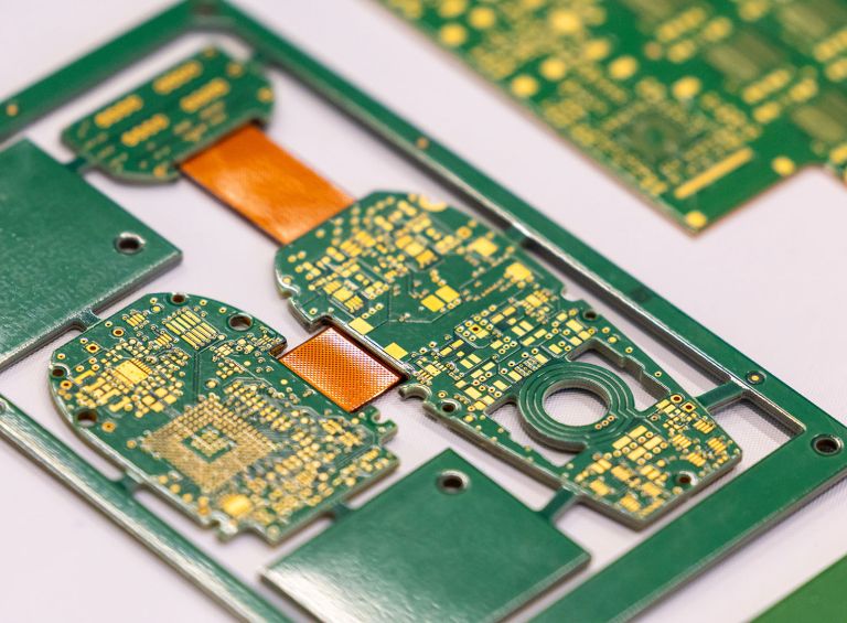
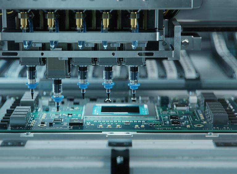
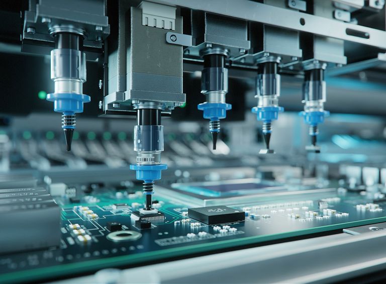
This course is designed to provide the skills necessary to effectively implement designs requiring flex and rigid-flex circuits in accordance with product requirements. PCB Design for Flex & Rigid-Flex Boards also focuses on the impact of these designs on manufacturing and assembly techniques, documentation, and manufacturing file generation.

Equip yourself and your team with the knowledge and skills to design and layout PCBs that meet advanced signal integrity requirements, ensuring optimal performance in high-speed digital circuits.
How solder alloys are expected to perform in harsh environments will be summarized. Participants are encouraged to bring their own selected systems for deliberation.
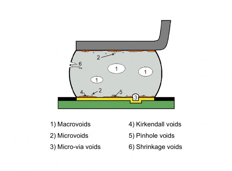
This course aims to enhance product reliability and maintain high production yields by offering comprehensive insights into solder joint voids. We will explore the origins of these voids, understand their causes, and analyze their impacts on solder joint efficacy and overall product dependability.
Discover practical solutions to common manufacturing challenges in the SMT process. Taught by Dr. Jennie Hwang, a globally recognized leader in electronics manufacturing and reliability, this course delves into the root causes of solder joint and assembly defects and provides actionable strategies to prevent them. Ideal for professionals seeking to enhance yield, reduce costs, and ensure product reliability, Module 1 equips participants with real-world insights and engineering principles to tackle production floor issues effectively.
Gain practical knowledge and actionable strategies for preventing and resolving production floor defects. By examining the root causes and contributing factors of common defects, this course focuses on manufacturing challenges related to bare PCBs, PCB fabrication, and components.
The Transform Your Constraint Engineering PCB Designs course is developed to provide specific paths to understanding Electrical and Mechanical Models which allows the experienced PCB design engineer opportunities to generate specific routing features to help improve, develop, and advance their design skills into a robust engineering skill set.
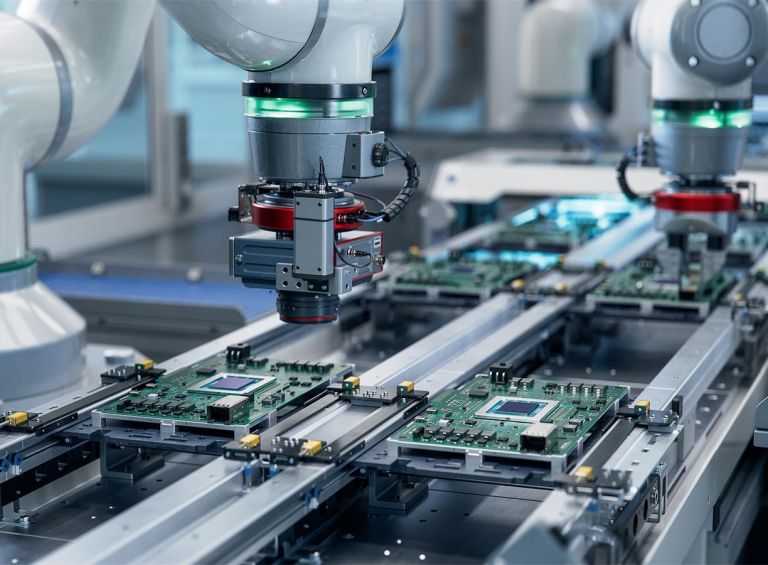
Equip your team to quickly and effectively identify, analyze, and address PCBA production defects. Jim Hall and Phil Zarrow, the authors of Troubleshooting for Electronics Manufacturing and the acclaimed BoardTalk podcast, offer decades of practical insights that students can immediately use to increase reliability, yields, and cost savings.